Our engineering focus
The packaging problems we design for — from the 300mm quantum platform and advanced interconnects to design-for-test and PDK-aligned layouts.
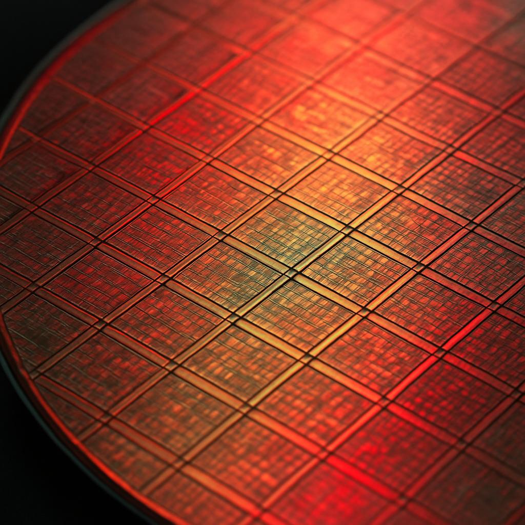
The packaging problems we design for
Getting quantum behaviour out of silicon is genuinely hard. The interconnects have to be dense, the signal integrity preserved, and the tolerances tighter than anything classical chips demand. That is the space our design work lives in.
Because packaging design is all we do, we can put our full attention there — and hand each client a design their foundry can build with confidence.
Where our design work goes deep
- 01
The 300mm Quantum Platform
We design toward the 300mm quantum wafer — the substrate the next generation of quantum hardware is built on. Understanding its constraints shapes every layout we produce.
- 02
Through-Silicon Vias (TSV)
We design vertical interconnects that pass directly through the silicon, enabling the dense, high-performance 3D integration that classical packaging cannot match.
- 03
Wafer-Scale Bumping
We lay out bumping across the full wafer to reach the interconnect density and reliability production-grade quantum devices demand.
- 04
Design-for-Test
We design so wafers can be measured and characterized in-line at your foundry, so the data you need to refine a design surfaces early rather than at the end.
- 05
PDK-Aligned Layouts
We draw every design against your foundry’s Process Design Kit, so what we hand over is genuinely manufacturable and ready to build.